Korea’s Largest Semiconductor Complex in Yongin 2026
Korea’s largest semiconductor complex is advancing rapidly in Yongin, South Korea.
It integrates industrial operations, architectural design, and urban infrastructure.
Upon completion in 2026, it will become the world’s largest semiconductor manufacturing facility.
It links fabrication plants with logistics networks, skilled labor, and regional transport.

Official Approval and Urban Planning
South Korea’s Ministry of Trade, Industry and Energy confirmed the project will stay at its current site.
Officials ruled out relocation.
They prioritized industrial water, high capacity electricity, and support services.
The complex anchors the national semiconductor supply chain through cities planning principles.
Urban integration is not optional for next-generation industrial sites it is foundational.
Engineering and Electrical Challenges
The complex demands about 15 gigawatts of power equal to 15 nuclear reactors.
Engineers designed a dedicated grid with natural gas stations and high voltage lines.
Teams focused civil and industrial construction on uninterrupted operation.
Long-term sustainability guides every technical decision.
Site Integration and Industrial Layout
Planners chose Yongin for its access to Seoul’s workforce and transport routes.
They wove production zones into residential areas using dedicated logistics paths.
This reflects core architectural design strategies that balance efficiency with future growth.
Korea’s largest semiconductor complex embeds this logic into road alignments, utility corridors, and spatial sequencing.
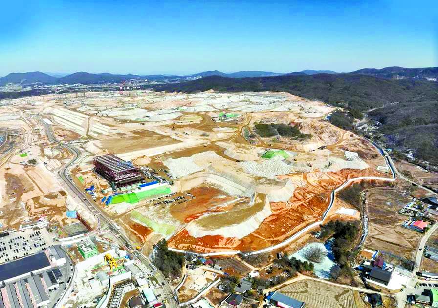
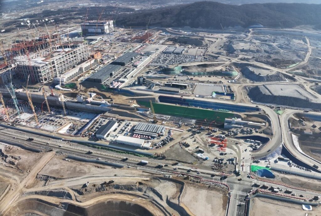
Construction Progress and Architectural Infrastructure
Developers plan ten fabrication plants four from SK Hynix and six from Samsung.
Work on the first SK Hynix plant started in February 2025.
The campus includes R&D labs, storage units, and production lines.
Designers optimized all spaces for environmental performance.
Over 80 specialized organizations now operate onsite.
This positions the project as a global benchmark in the archive.
Teams selected high performance building materials and modular systems.
By 2026, Korea’s largest semiconductor complex will function as both an industrial hub and an urban prototype.
Industrial scale no longer excuses spatial disorder; precision defines modern manufacturing landscapes.
Architectural Snapshot
Korea’s largest semiconductor complex demonstrates how industrial architecture can function as urban infrastructure when guided by spatial intelligence and systemic planning.
✦ ArchUp Editorial Insight
The article frames Yongin’s campus as engineering meeting urbanism.
It relies on official data and precise spatial facts.
But it skips hard questions: Who pays the ecological price?
Can massive scale excuse visual silence?
Its strength is rare clarity on infrastructure and logistics.
It may last as a technical record.
Not as a visionary statement.