Light That Is Built, Not Simply Cast

How Architectural Facades Are Becoming Optical Circuits That Redirect Natural Light With Nanometric Precision
There is a question that has lingered, unasked with any real precision, in architectural discourse for decades: can light function as a building material? Not in the poetic sense that architects invoke when they speak of “the play of light and shadow,” but in the strict engineering sense — light that is redirected, shaped, and distributed with the same deliberateness applied to a structural beam or a mechanical duct. That is precisely what a convergence of research published across Nature Photonics and Nature Reviews Electrical Engineering over the past three years now proposes, tracing the contours of a technology known as programmable photonic waveguide arrays — integrated circuits through which light travels along paths that can be reconfigured in fractions of a second, rather than paths fixed immutably at the moment of fabrication.
What remains absent from both industry and academic conversation is the recognition that this technology does not belong exclusively to optical communications laboratories or quantum computing hardware. At its core, it addresses an architectural question as old as the discipline itself: how do we govern the movement of light through the built space?
From Waveguide to Wall: The Logic of Structural Analogy
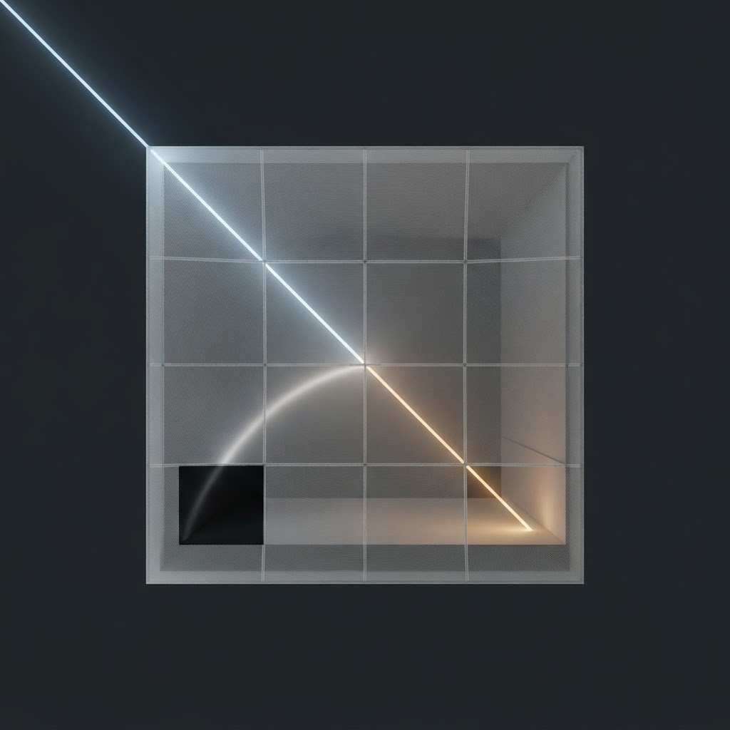
Understanding what this technology means for architecture requires no fluency in quantum optics — only familiarity with its operational logic. A photonic waveguide is a nanoscale conduction channel through which a light wave travels as water moves through a pipe: contained, directed, neither leaking nor scattering. What researchers have achieved is the weaving of thousands of such channels into interconnected networks that intersect at small “optical gates,” each gate governing the proportion of light that continues forward and the proportion that deflects. When the electrical signal reaching those gates changes, the entire network changes its function — without any change to its physical substance.
The foundational reference document in this body of work — prepared by Bogaerts, Pérez, Capmany, Miller, and colleagues and published in Nature in 2020 under the title “Programmable Photonic Circuits” — establishes that a waveguide mesh can execute any linear transformation between its inputs and outputs, reconfiguring itself as a signal distributor, a spectral filter, or a matrix multiplier, all without touching the material and without returning to the fabrication stage.
This is precisely where the structural analogy with the building envelope holds. A conventional glass facade is a fixed-function element: transparent or opaque, reflective or absorptive. An envelope built on programmable photonic circuits could function as a direct-light filter in the morning, a diffuse-light distributor at midday, and a thermal reflector in the afternoon — more effectively than any conventional glass coating — and all of this through an electrical signal, without manual intervention and without reconstruction.
Sculpted Light: When the Facade Becomes a Generator of Architectural Illumination
In 2024, Nature Photonics published a study led by Bütow, Eismann, Sharma, and Banzer demonstrating that a chip-scale programmable waveguide mesh can produce structurally complex light beams — known in optics as Hermite-Gaussian and Laguerre-Gaussian modes — with complete flexibility and no moving parts. These patterns are not academic abstractions; they are simply light given a programmable geometric form: concentric rings, interlocking grids, a beam inclined at a specified angle, or illumination distributed uniformly across an entire surface.
What this means architecturally is the capacity to sculpt natural light — reflected or filtered through the facade — with nanometric spatial precision. The designer would not place a canopy, a light diffuser, or a reflective panel. Instead, a mathematical equation would determine how incoming optical energy distributes itself across the interior volume.
More significantly, the same study indicates that configuring the mesh requires no complex machine-learning algorithms — a single initial calibration followed by direct computation is sufficient. That means such a facade could be managed by a conventional Building Management System (BMS) rather than a dedicated computing facility.
Thermal Load and the Cost of Stasis: The Sustainability Argument
Among the most consequential findings in this body of research, from a thermal sustainability standpoint, is the property known as non-volatile reconfiguration. A class of phase-change materials can retain their optical state — absorptive or reflective — without any continuous energy draw. The facade is updated once in the morning and holds that configuration until the next scheduled update in the evening, consuming no power during the intervening hours.
This distinguishes the approach fundamentally from current electrochromic glazing systems, which require continuous current to maintain a tinted state. When combined with the networks’ demonstrated capacity to direct incoming light toward specific zones within the interior volume — rather than dispersing it across the entire surface — it becomes possible for the north-facing corner of an office to receive the natural daylight that conventional reflective glazing would otherwise waste entirely.
Research on optical phased arrays — reviewed by Xu, Yuan, and colleagues in npj Nanophotonics in 2025 — records that every three decibels of optical loss translates into approximately a thirty percent reduction in system performance. The parallel with building envelope physics is precise: this relationship mirrors the function of the thermal transmittance coefficient (U-value) in energy performance research. Light dissipated within the conductive network is energy that never reaches the occupied space, in the same way that heat escapes through thermal bridges in a structural frame.
The Topological Network: When the Building Is Fault-Tolerant by Design
Among the concepts that bring this technology closest to genuine architectural application — rather than confining it to laboratory demonstration — is the work on topological waveguide arrays documented by Song, Sun, Chen, and colleagues in Laser and Photonics Reviews in 2020. Topology in the photonic context means that the light wave travels along “protected” paths that remain operative even when manufacturing defects or structural deviations reach twenty-six percent of original specifications. Performance did not degrade appreciably under those conditions; the networks retained more than ninety percent of their efficiency and delivered a bandwidth approximately ten times wider than that of conventional couplers.
Translated into architectural terms, this describes an envelope whose performance does not fail when its glazing expands thermally, when dust accumulates on certain control gates, or when a segment of the sensor network malfunctions. The topological system absorbs these failures structurally, because the light path depends not on the precision of each individual gate but on the collective logic of the network.
For building envelope designers, this is not a technical detail — it is the reliability condition that determines whether any system can move from a peer-reviewed paper into a construction document.
Engineering Challenges: What Stands Between the Laboratory and the Site
The story does not end with capabilities. What separates this technology from widespread architectural application is a set of genuine engineering challenges that practitioners should read with critical attention rather than premature skepticism.
The first is optical loss. Each switching gate in the network absorbs between 0.05 and 0.2 decibels of optical energy, and those losses accumulate along the full length of the light path. In an architectural application that may extend across facade panels measuring tens of square meters, this accumulation complicates the design and imposes a practical ceiling on the size of any network that can operate effectively. The direction researchers are currently pursuing is the use of low-loss silicon nitride waveguides, combined with the heterogeneous integration of gain materials that compensate for optical depletion.
The second challenge is thermal crosstalk. Most control elements in current networks rely on localized heating to modify wave propagation characteristics, which produces thermal leakage between adjacent network elements that disrupts calibration accuracy. In the environment of an architectural facade — subject to daily external thermal differentials of twenty to thirty degrees Celsius — this thermal sensitivity is not acceptable in its current form without additional treatment.
The third challenge, and the most complex from a systems engineering perspective, is calibration. Managing thousands of actuators within a single network to produce a predetermined light distribution is an inherently nonlinear computational problem, requiring algorithms that continuously self-correct. Research overseen by Wang Lishu and published in Nature Reviews Electrical Engineering in 2024 demonstrated that deploying two matched waveguide mesh chips in opposition, governed by an iterative optimization algorithm, can achieve inter-channel crosstalk below minus thirty decibels — a level sufficient for precise operation in variable optical environments, but one that demands processing time and computing power that cannot be dismissed.
From Laboratory Prototype to Construction Site: A Technology Roadmap
These challenges notwithstanding, the technology advances along a clear trajectory. The increasing integration of low-loss optical waveguides, high-speed electro-optic phase materials, and three-dimensionally stacked electronic drivers is currently described — in the comprehensive review by Xu and colleagues published in 2025 — as “the most realistic route toward large coherent apertures.” That formulation carries architectural weight.
From a design perspective, it means that a system currently demonstrable only on a chip a few square centimeters in area is moving, at measurable pace, toward configurations capable of covering standard facade panels. Any architect working today with dynamic glazing or intelligent shading systems should register this technology within the planning horizon of the coming decade.
What merits particular attention is that this technology does not add a new function on top of the existing envelope — it redefines what the envelope itself is. Instead of stacked layers of glass, mesh, canopy, and sensor, the envelope becomes an integrated circuit that carries within its own material structure the capacity to respond, adapt, and be reprogrammed. That shift from accumulated layers to a unified system is precisely what the field-programmable gate array (FPGA) accomplished in electronics: decoupling function from fabrication, and relocating innovation from hardware construction to software configuration. Programmable waveguide arrays hold the same prospect for architecture.
✦ ArchUp Editorial Insight
The article under analysis presents programmable photonic waveguide arrays as an architectural frontier, and the framing is structurally accurate — but the more consequential question is not whether this technology can redirect light with nanometric precision, but rather who controls the reconfiguration protocol, and at what point in the procurement chain that control is assigned. The building envelope has historically been the site where responsibility is most aggressively subdivided: the glazing contractor is not the thermal performance consultant, who is not the building services engineer, who is not the facilities manager who will operate the system for the next thirty years under a maintenance budget set before the technology existed. Programmable photonic envelopes introduce a new layer into this already fractured accountability chain — a software layer, owned by a manufacturer, updated at the manufacturer’s discretion, and licensed rather than purchased — which means the building owner acquires a facade whose long-term optical behavior is governed by a subscription agreement, not a construction specification. The structural parallel this archive identified in Architectural Design for Twenty Dollars applies with equal force here: when the intelligence of a building system is extractable intellectual property rather than embedded material knowledge, the lock-in is not a technical inconvenience but a deliberate revenue architecture, and the liability for system failure after a license lapses, a firmware update miscalibrates, or a manufacturer exits the market transfers entirely to the party with the least negotiating power and the longest exposure — which is, as this pattern consistently resolves, the occupant.
References
Bütow, J., Eismann, J.S., Sharma, V., Brandmüller, D., and Banzer, P. “Generating Free-Space Structured Light with Programmable Integrated Photonics.” Nature Photonics, 2024.
Farmakidis, N., Dong, B., and Bhaskaran, H. “Integrated Photonic Neuromorphic Computing: Opportunities and Challenges.” Nature Reviews Electrical Engineering, 2024.
Aharonovich, I., Crozier, K.B., and Neshev, D. “Programmable Integrated Quantum Photonics.” Nature Photonics, 2026.
Wang, Lishu. “Interferometer Meshes for Low-Crosstalk Scalable Optical Chips.” Nature Reviews Electrical Engineering, 2024.
Pérez, D., Gasulla, I., Capmany, J., and Soref, R.A. “Reconfigurable Lattice Mesh Designs for Programmable Photonic Processors.” Optics Express, 2016.
Garanovich, I.L., Szameit, A., Sukhorukov, A.A., Pertsch, T., Krolikowski, W., Nolte, S., Neshev, D., Tünnermann, A., and Kivshar, Y.S. “Diffraction Control in Periodically Curved Two-Dimensional Waveguide Arrays.” Optics Express, 2007.
Bogaerts, W., Pérez, D., Capmany, J., Miller, D.A.B., Poon, J., Englund, D., Morichetti, F., and Melloni, A. “Programmable Photonic Circuits.” Nature, 2020.
Xu, W., Yuan, Q., Yang, Y., Lu, L., Chen, J., and Zhou, L. “Progress and Prospects for LiDAR-Oriented Optical Phased Arrays Based on Photonic Integrated Circuits.” npj Nanophotonics, 2025.
Guo, Y., Guo, Y., Li, C., Zhang, H., Zhou, X., and Zhang, L. “Integrated Optical Phased Arrays for Beam Forming and Steering.” Applied Sciences, 2021.
Kang, J., Wei, R., Zhang, Q., and Dong, G. “Topological Photonic States in Waveguide Arrays.” Advanced Physics Research, 2022.
Song, W., Sun, W., Chen, C., Song, Q., Xiao, S., Zhu, S., and Li, T. “Robust and Broadband Optical Coupling by Topological Waveguide Arrays.” Laser and Photonics Reviews, 2020.